Note: Descriptions are shown in the official language in which they were submitted.
WO 2021/159214
PCT/CA2021/050155
HIGH PERFORMANCE PEROVSKITE SOLAR CELLS, MODULE DESIGN, AND MANUFACTURING
PROCESSES THEREFOR
CROSS-REFERENCE TO RELATED APPLICATIONS
This application claims priority to and the benefit of the filing of U.S.
Provisional Patent No.
62/975,590, entitled "High Performance Perovskite Solar Cells, Module Design,
and Manufacturing
Processes Therefor", filed on February 12, 2020, the entirety of which is
incorporated herein by reference.
BACKGROUND OF THE INVENTION
Field of the Invention (Technical Field)
The present invention is related to high performance flexible perovskite solar
cells (PSCs) and
flexible/stretchable PSC modules that take advantage of high-throughput
manufacturing processes.
Backoround Art
Note that the following discussion may refer to a number of publications and
references.
Discussion of such publications herein is given for more complete background
of the scientific principles
and is not to be construed as an admission that such publications are prior
art for patentability
determination purposes.
Conventional solar cells are made from brittle crystalline semiconductors that
crack when flexed.
Some solar cell materials, including many PSC materials, exist that are
flexible to a certain degree. PSCs
can be manufactured using all-low-temperature processing (below 150 deg C)
that allows the cells to be
fabricated on flexible substrates. The fabrication of flexible PSCs is well
known in the art, although a
method for manufacturing PSC modules that can form-fit to complex, or organic,
contoured surfaces is
still lacking. In order to accomplish this novel application of PSCs, a degree
of stretch can be integrated
into the PSC module design.
PSCs suffer from high series resistance due to the high sheet resistance of
transparent
conductive oxides (TC0). To reduce this series resistance perovskite cells are
typically series connected
via sequential laser scribing and deposition processes, or by depositing an
underlayer of metal on the
-1-
CA 03167998 2022- 8- 12
WO 2021/159214
PCT/CA2021/050155
TOO. Both of these methods for reducing series resistance are well known in
the art. Although these
methods reduce the series resistance of the TOO, neither method can be
incorporated into a module
design that can be flexible in more than one direction or that is stretchable,
both of which features (at
least 1 degree of flex and at least 1 degree of stretch) are necessary to form-
fit to organic contours. The
development of stretchable conductive interconnects is well known in the art,
but a design for
interconnecting PSCs into a flexible/stretchable module is lacking.
In order to facilitate the growing potential of solar as an economical
alternative to fossil-fuels, the
potential applications must grow. A largely untapped industry for solar
implementation is the auto
industry. The auto industry is responsible for 23% of CO2 gas emissions and
20% of energy use
worldwide. The electric vehicle (EV) market aims to substitute electric
alternatives to fossil-fuel based
engines. The key advantage to electric powered engines is that the batteries
that power the car can be
recharged using sustainable sources of energy, leading to a potential global
reduction in CO2 production.
In order to increase the feasibility of solar EV's, the portion of a vehicle's
surface which a solar panel can
be applied to must increase, and consequently, the solar module must shape to
the complex 'organic'
contours that are common in modern automobile design. To facilitate this
design requirement, solar
modules must be flexible in more than one direction, and stretchable in at
least one direction.
SUMMARY OF THE INVENTION (DISCLOSURE OF THE INVENTION)
An embodiment of the present invention is a flexible and stretchable solar
module comprising a
first flexible perovskite solar cell and a second flexible perovskite solar
cell disposed on a stretchable
substrate; and a deformable interconnect electrically connecting the first
flexible perovskite solar cell and
second flexible perovskite solar cell. The stretchable substrate preferably
comprises polydinnethylsiloxane
(PDMS) or vinyl. The solar module is preferably capable of conforming to a
contoured surface of an
object. Each of the solar cells preferably comprises a flexible substrate
coated with a transparent
conductive oxide (TOO) layer, which is preferably selected from the group
consisting of indium tin oxide
(ITO), silver nanowires, single-layer graphene, graphene nanoplates, and
combinations thereof.
Preferably an exposed portion of the TOO layer on each solar cell is not
covered by overlaying layers of
the solar cell. Each of the solar cells was preferably manufactured using slot-
die coating. The exposed
portion of the TOO layer is between approximately 1 pm and approximately 10mm
wide, more preferably
-2-
CA 03167998 2022- 8- 12
WO 2021/159214
PCT/CA2021/050155
approximately 1mm wide. Each solar cell preferably comprises a metal contact
disposed on at least a part
of the exposed portion of the TCO layer. The metal contact was preferably
disposed on the exposed
portion of the TCO layer by metal evaporation using a mask, screen printing,
or attaching the metal
contact to the exposed portion of the TCO layer with an electrically
conductive adhesive tape. The
exposed portion of the TCO layer is optionally formed by removing the
overlaying layers over the exposed
portion of the TCO layer by mechanical etching or laser scribing. The
overlaying layers preferably
comprise an electron transport layer (ETL), a perovskite layer, a hole
transport layer (HTL), and a
conductive layer. The deformable interconnect can electrically connect the
metal contact on the first
flexible perovskite solar cell to the metal contact on the second flexible
perovskite solar cell, the
conductive layer on the first flexible perovskite solar cell to the conductive
layer on the second flexible
perovskite solar cell, and/or the metal contact on the first flexible
perovskite solar cell to the conductive
layer on the second flexible perovskite solar cell.
The deformable interconnect preferably is flexible and/or stretchable. In some
embodiments a
portion of the stretchable substrate preferably extends vertically between the
first flexible perovskite solar
cell and the second flexible perovskite solar cell. The portion of the
stretchable substrate is preferably
between about 1 mm and about 10 mm in width and preferably comprises a wavy
surface. A first side of
the wavy surface is preferably approximately adjacent to a first contact on
the first flexible perovskite solar
cell and a second side of the wavy surface is preferably approximately
adjacent to a second contact on
the second flexible perovskite solar cell. In this case the deformable
interconnect preferably comprises a
layer of conductive material deposited on the wavy surface, thereby
electrically connecting the first
contact and the second contact Alternatively, the deformable interconnect
comprises a coiled metal wire,
a hinged metal wire, a flexible and/or stretchable conductive contact, or a
hinged metal connector. The
solar module preferably further comprises a stretchable cover layer
encapsulating the first flexible
perovskite solar cell, the second flexible perovskite solar cell, and the
deformable interconnect.
In some embodiments the deformable interconnect preferably comprises a
conductive paste
disposed between the first flexible perovskite solar cell and the second
flexible perovskite solar cell. The
conductive paste preferably electrically connects the exposed portion of the
TCO on the first flexible
perovskite solar cell and the exposed portion of the TCO on the second
flexible perovskite solar cell. The
exposed portion of the TCO layer on the first flexible perovskite solar cell
and the exposed portion of the
-3-
CA 03167998 2022- 8- 12
WO 2021/159214
PCT/CA2021/050155
TCO layer on the second flexible perovskite solar cell preferably spatially
overlap but are preferably not in
physical contact. For each of the solar cells, perovskite forming a perovskite
layer is preferably extended
to electrically insulate from the conductive paste those layers of the solar
cell which are not adjacent to
the TCO layer. In serially connected embodiments the order of layers in each
solar cell is preferably the
same, but the exposed portion of the TCO layer in the first flexible
perovskite solar cell is preferably
facing downward from a top portion of the first flexible perovskite solar cell
and the exposed portion of the
TCO layer in the second flexible perovskite solar cell is preferably facing
upward from a bottom portion of
the second flexible perovskite solar cell. In parallel connected embodiments
the first flexible perovskite
solar cell is preferably inverted on the stretchable substrate with respect to
the second flexible perovskite
solar cell so that the positions of an HTL and an ETL in the first flexible
perovskite solar cell are preferably
exchanged with respect to positions of an HTL and an ETL in the second
flexible perovskite solar cell.
The solar module preferably further comprises a stretchable layer covering the
first flexible perovskite
solar cell, the second flexible perovskite solar cell, and the conductive
paste, and is preferably conformed
to a contoured surface prior to curing of the conductive paste.
An embodiment of the present invention is a method of manufacturing a flexible
and stretchable
solar cell, the method comprising: producing first and second flexible
perovskite solar cells, each cell
comprising an exposed portion of a TCO layer on a bottom of the solar cell and
a conductive layer on the
top of the solar cell; disposing a metallic contact on at least a part of
exposed portion of the TCO layer on
each of the solar cells; placing the first flexible perovskite solar cell and
the second flexible solar cell on a
stretchable substrate; and electrically connecting the first flexible
perovskite solar cell and the second
flexible solar cell with a deformable interconnect. The stretchable substrate
preferably comprises PDMS
or vinyl. The producing step preferably comprises slot-die coating, or
alternatively comprises removing
layers overlaying the TCO layer using mechanical etching or laser scribing to
produce the exposed
portion of the TCO layer on each of the flexible perovskite solar cells. The
electrically connecting step
preferably comprises connecting the metal contact on the first flexible
perovskite solar cell to the metal
contact on the second flexible perovskite solar cell, connecting the
conductive layer on the first flexible
perovskite solar cell to the conductive layer on the second flexible
perovskite solar cell, and/or connecting
the metal contact on the first flexible perovskite solar cell to the
conductive layer on the second flexible
perovskite solar cell. In some embodiments the placing step preferably
comprises indenting the first
-4-
CA 03167998 2022- 8- 12
WO 2021/159214
PCT/CA2021/050155
flexible perovskite solar cell and the second flexible perovskite solar cell
into the stretchable substrate
prior to curing of the stretchable substrate so that a portion of the
stretchable substrate extends vertically
between the first flexible perovskite solar cell and the second flexible
perovskite solar cell. The method
preferably comprising producing a wavy pattern on a surface of the portion of
the stretchable substrate,
preferably by stamping, chemical etching, or molding. The electrically
connecting step preferably
comprises depositing a layer of conductive material on the wavy-patterned
surface of the portion of the
stretchable substrate, thereby connecting a contact on the first flexible
perovskite solar cell with a contact
on the second flexible perovskite solar cell. The method preferably further
comprises encapsulating the
first flexible perovskite solar cell, the second flexible perovskite solar
cell, and the deformable
interconnect in a stretchable cover layer. The disposing step preferably
comprises metal evaporation
using a mask, screen printing, or attaching the metal contact to the portion
of the TCO layer with an
electrically conductive adhesive tape.
In other embodiments the electrically connecting step preferably comprises
disposing a
conductive paste between the first flexible perovskite solar cell and the
second flexible perovskite solar
cell. The conductive paste preferably electrically connects the exposed
portion of the TCO on the first
flexible perovskite solar cell and the exposed portion of the TCO on the
second flexible perovskite solar
cell. The method preferably comprises spatially overlapping but not directly
contacting the exposed
portion of the TCO on the first flexible perovskite solar cell and the exposed
portion of the TCO on the
second flexible perovskite solar cell. The placing step optionally comprises
inverting the first flexible
perovskite solar cell with respect to the second flexible perovskite solar
cell The method preferably
further comprises covering the solar module with a stretchable cover layer;
conforming the solar module
to a contoured surface of an object; and curing the conductive paste.
Objects, advantages and novel features, and further scope of applicability of
the present invention
will be set forth in part in the detailed description to follow, taken in
conjunction with the accompanying
drawings, and in part will become apparent to those skilled in the art upon
examination of the following, or
may be learned by practice of the invention. The objects and advantages of the
invention may be realized
and attained by means of the instrumentalities and combinations particularly
pointed out in the appended
claims.
-5-
CA 03167998 2022- 8- 12
WO 2021/159214
PCT/CA2021/050155
BRIEF DESCRIPTION OF THE DRAWINGS
The accompanying drawings, which are incorporated into and form a part of the
specification,
illustrate the practice of embodiments of the present invention and, together
with the description, serve to
explain the principles of the invention. The drawings are only for the purpose
of illustrating certain
embodiments of the invention and are not to be construed as limiting the
invention. In the drawings:
FIG. 1 is a schematic showing the PSC device architecture after
interconnection using method 1,
where the interconnect is preferably a layer of conductive material deposited
on the stretchable carrier
substrate.
FIG. 2 shows the manufacturing process of PSCs including the steps required to
prepare the
substrate for interconnection.
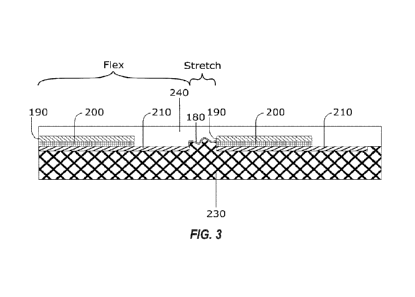
FIG. 3 shows the interconnection scheme in more detail where the perovskite
cell is positioned on
a stretchable underlayer that has been molded in the connection region. The
conductive material contact
is then deposited on the wavy stretchable region interconnecting the
individual cells. Finally, an
encapsulating layer of stretchable material is coated on top of the conductive
contact.
FIG. 4A shows an interconnection scheme for series connections.
FIG. 4B shows an interconnection scheme for parallel connections.
FIG. 5A shows the interconnection before bending and stretching.
FIG. 5B shows the interconnection after bending and stretching. The perovskite
cell on the
flexible substrate can bend, and the electrical interconnect can bend and
stretch.
FIG 6 shows an alternative embodiment of the present invention where the
interconnect is
preferably formed using a conductive paste to electrically connect adjacent
cells serially.
FIG. 7 shows a module similar to that of FIG. 6 after bending and stretching.
The perovskite cell
on the flexible substrate can bend, and the stretchable substrate/electrical
interconnect can bend and
stretch.
FIG. 8 shows the alternative embodiment of the present invention where the
interconnect is
preferably formed using a conductive paste to electrically connect adjacent
cells in parallel.
FIGS. 9A-9B show several examples of complex, or 'organic', contours that
require more than
one degree of bend, and at least one degree of stretch to form-fit a coating
on the surface. FIG. 9A shows
-6-
CA 03167998 2022- 8- 12
WO 2021/159214
PCT/CA2021/050155
an example of a 2-axis organic contour. FIG. 9B shows an application
comprising two dimensional
organic contours.
DETAILED DESCRIPTION OF EMBODIMENTS OF THE INVENTION
Embodiments of the present invention are arrays of interconnected photovoltaic
PCSs. The PSCs
preferably comprise a narrow strip of flexible PSC that has been cut from a
larger PSC that preferably has
been manufactured using high throughput roll-to-roll manufacturing processes.
The cells are each
preferably between about 1mm and lOmm wide, and their length is preferably
between about 1cm and
1m. Each cell is preferably sufficiently narrow to accommodate the design
constraints of the contour that
it will be applied to. Two embodiments of the present invention are methods of
manufacturing stretchable
interconnections for PSCs enabling them to cover complex contoured surfaces.
The present invention
provides several valuable improvements to solar module structures, including
the combination of flexible
solar cells interconnected into an array of series and/or parallel connected
cells using flexible and
stretchable mechanical/conductive interconnections, as well as using high
throughput manufacturing
techniques to fabricate the solar cells and solar modules. The preferable
flexible and/or stretchable
interconnection of thin strips of PSCs embedded in a flexible carrier
substrate both reduces the inherent
series resistance in the PSCs and increases the deformability of the module.
This design results in the
potential to form-fit a solar module to complex organic contoured surfaces.
FIG. 1 illustrates an exemplary device architecture of two PSCs connected in
series constructed
in accordance with a first embodiment of the present invention Each PSC
preferably comprises flexible
carrier substrate 150, transparent conductive oxide (TOO) layer 140, electron
transport layer (ETL) 130,
perovskite layer 120, hole transport layer (HTL) 110, conductive layer 100,
and electrical contact 160 on
TOO layer 140. FIG. 2 shows an example of the fabrication steps for the device
shown in FIG. 1. First,
ETL 130 is deposited on carrier substrate 150 coated with at least one TOO
layer 140. Carrier substrate
150 may comprise any material, including but not limited to polyethylene
terephthalate (PET). TOO layers
140 may comprise, for example, indium tin oxide (ITO), silver nanowires,
single-layer graphene, graphene
nanoplates, and/or combinations thereof, together with carrier substrate 150
preferably forming a
transparent, flexible, and conductive composite substrate. ETL 130 may
comprise any material, including
but not limited to a transition metal oxide such as TiO2, Sn02, ZnO, 111203,
G2203, or CdO, and may be
-7-
CA 03167998 2022- 8- 12
WO 2021/159214
PCT/CA2021/050155
deposited by a method such as spin-coating, slot-die coating, air-blade
coating, doctor-blade coating,
sputtering, e-beam evaporation, or chemical bath deposition, in which any heat
treatment does not
exceed the melting temperature of the carrier substrate 150 or TCO layer 140.
Perovskite layer 120 is
then preferably deposited on ETL 130 by a method such as spin-coating, slot-
die coating, air-blading,
spray-coating, or blade-coating, which method preferably does not comprise a
heat treatment exceeding
the melting temperature of any of the underlying layers. Perovskite layer 120
preferably comprises the
ABX3 structure, where A is a cation comprising, for example, nnethylammonium,
formamidinium, cesium,
or rubidium; B is a cation comprising, for example, lead or tin; and X is an
anion comprising, for example,
an iodide, bromide or chloride. HTL 110 is then preferably deposited on
perovskite layer 120 by a
method such as spin-coating, slot-die coating, air-blading, spray-coating, or
blade-coating, which method
preferably does not comprise a heat treatment exceeding the melting
temperature of any of the
underlying layers. HTL 110 preferably comprises 2,2',7,7'-Tetrakis[N,N-di(4-
methoxyphenyl)amino]-9,9'-
spirobifluorene (spiro-OMeTAD), [6,6]-phenyl 061 butyric acid methyl ester
(PCBM), or a graphite slurry
that includes additives such as carbon black to increase the conductivity. If
HTL 110 is not sufficiently
conductive, optional conductive layer 100 may be deposited on HTL 110 for
forming the top electrical
contact to the PSC.
The PSCs of the present invention are preferably processed in strips that
provide access to both
the top contact (conductive layer 100) and bottom contact (TCO layer 140),
i.e., leaving strip 170 of TCO
layer 140 uncovered by ETL 130, perovskite layer 120, HTL 110, and conductive
layer 100. This is
preferably accomplished by processing ETL 130, perovskite layer 120, HTL 110,
and conductive layer
100 in strips using slot-die coating, which can be configured to leave strip
170 of TCO-coated carrier
substrate 150 uncoated. Alternatively, mechanical etching or laser scribing
can be used to remove ETL
130, perovskite layer 120, HTL 110, and conductive layer 100 to create strip
170. Strip 170 is preferably
approximately between 1 pm and lOmm wide, and more preferably about lmm wide.
Electrical contact
160 is then deposited or attached to a portion of uncovered strip 170 of TCO
layer 140 to form the bottom
electrical contact to the PSC. Electrical contact 160 is preferably disposed
on TOO layer 140 using a
method including but not limited to metal evaporation using a mask, screen
printing, or attaching the
contact via an electrically conductive adhesive tape. Stretchable
interconnection 180, which is preferably
also flexible, is formed between electrical contact 160 and optional
conductive layer 100.
-8-
CA 03167998 2022- 8- 12
WO 2021/159214
PCT/CA2021/050155
As shown in FIG. 3, the cells are then placed on a stretchable substrate 230,
which preferably
comprises polydimethylsiloxane (PDMS). In FIG. 3, to simplify the drawing,
layer 190 represents optional
conductive layer 100, layer 200 represents ETL 130, perovskite layer 120, and
HTL 110, and layer 210
represents carrier substrate 150 coated with TCO layer 140, including uncoated
strip 170 and electrical
contact 160. The gap between the cells is preferably between about 1 mm and
about 10 mm. In this gap,
stretchable substrate 230 preferably extends above layer 210 and layer 200,
and its surface preferably
comprises a wavy pattern such as that shown in FIG. 3. The wavy pattern may be
produced by a method
such as stamping, chemical etch, pouring the stretchable substrate into a
mold, or by any other means.
The height of the stretchable substrate in the gap is preferably extended
above the cells by laying down
the cells on the stretchable substrate when it is soft before curing and
pressing the cells down.
Stretchable interconnection 180 preferably comprises a thin layer of
conductive material, preferably
between approximately 1 nm and 1000 nm in thickness, that is preferably
deposited on electrical contact
160 on the uncoated TOO strip 170 (shown in FIGS. 1-2) and the wavy surface of
that portion of the
stretchable substrate in the gap between adjacent cells. Alternatively,
stretchable interconnection 180
may comprise a coiled or hinged metal wire, a flexible and/ or stretchable
conductive contact, or a hinged
metal connector. Stretchable interconnection 180 connects the cell to the
adjacent solar cell either in
series or in parallel, depending on the voltage and current specifications
required for the application. Such
an interconnect enables the module to stretch and bend between adjacent
flexible perovskite solar cells
without stressing/breaking the metal interconnect. To encapsulate the
contacts, top stretchable layer 240,
preferably comprising a material such as PDMS, is deposited using at least one
of spin-coating, slot-die
coating, drop-casting, or blade-coating.
FIGS. 4A and 4B show series and parallel interconnections of PSCs
respectively. As shown in
FIG. 4A, for a series connection the stretchable interconnect is connected
between the top contact
(conductive layer 100) and the bottom contact (TOO layer 140) of adjacent
flexible perovskite solar cells.
For parallel connection, the stretchable interconnect is connected between
adjacent flexible perovskite
solar cells twice, where one connection is used to connect the top contacts of
adjacent cells and one is
used to connect the bottom contacts of adjacent cells, as shown in FIG 4B.
FIGS. 5A-5B illustrate a solar module of the present invention before and
after bending and/or
stretching, respectively, showing the resultant deformation of stretchable
interconnection 180. The
-9-
CA 03167998 2022- 8- 12
WO 2021/159214
PCT/CA2021/050155
perovskite solar module of the present invention is preferably flexible in at
least two directions and
stretchable in one or more directions. In this interconnection scheme, the
flexibility of the PSC itself
generates the first degree of bend, and the stretchable substrate and top
stretchable layer (not shown),
which comprises the encapsulated conductive interconnects, generates the
second degree of bend and
at least one degree of stretch.
FIG. 6 illustrates an alternative embodiment of the present invention
depicting a series
interconnection between two PSCs. Flexible substrate 260 preferably comprises
PET. TCO layer 270 is
preferably deposited on flexible substrate 260 to form one of the electrical
contacts of the PSC. TCO
layers 270 may comprise, for example, indium tin oxide (ITO), silver
nanowires, single-layer graphene,
graphene nanoplates, and/or combinations thereof, together with flexible
substrate 260 preferably forming
a transparent, flexible, and conductive composite substrate. ETL 280 may
comprise any material,
including but not limited to a transition metal oxide such as TiO2, Sn02, ZnO,
In203, Ga203, or CdO.
Perovskite layer 290 preferably comprises the ABX3 structure, where A is a
cation comprising, for
example, methylammonium, formamidinium, cesium, or rubidium; B is a cation
comprising, for example,
lead or tin; and X is an anion comprising, for example, an iodide, bromide or
chloride. HTL 300 preferably
comprises 2,2',7,T-Tetrakis[N,N-di(4-methoxyphenyl)amino]-9,9'-spirobifluorene
(spiro-OMeTAD), [6,6]-
phenyl C61 butyric acid methyl ester (PCBM), nickel oxide, or a graphite
slurry that includes additives
such as carbon black to increase the conductivity. IF HTL 300 is not
sufficiently conductive, conductive
layer 310, preferably comprising TCO similar to TCO layer 270, forms the other
electrical contact of the
PSC Conductive layer 310 is preferably covered by flexible layer 320 which
preferably comprises a
flexible, transparent material such as PET.
The PSCs in this embodiment preferably provide access to the top contact
(anode) and bottom
contact (cathode) of cells that are adjacent by leaving strips 360 and 370 of
TCO layer 270 and
conductive layer 310 exposed. This is preferably accomplished by processing
ETL 280, perovskite layer
290, HTL 300, conductive layer 310, and transparent flexible layer 320 in
strips using, for example, slot-
die coating, which can be configured to leave strips 360, 370 uncoated by the
subsequent layers.
Alternatively, mechanical etching or laser scribing can be used to remove ETL
280, perovskite layer 290,
HTL 300, conductive layer 310, and transparent flexible layer 320 to create
strips 360 and 370. Strips 360
and 370 are each preferably approximately between 1 pm and 10mnn wide, and
more preferably about
-10-
CA 03167998 2022- 8- 12
WO 2021/159214
PCT/CA2021/050155
1mm wide. The longer top contact (conductive layer 310) of the left cell is
then preferably electrically
connected to the longer bottom contact (TCO layer 270) of the adjacent right
cell via conductive paste
350, which preferably comprises silver, carbon, or any other material that can
form a conductive paste,
forming a series interconnection. Electrical isolation is preferably achieved
between the bottom contact
(TOO layer 270) of the left cell and top contact (conductive layer 310) of the
adjacent right cell by
configuring the deposition of perovskite layer 290 on each cell, which is
electrically insulating, to
electrically isolate the aforesaid layers from conductive paste 350. The
interconnection so formed thus
produces a series connection between adjacent cells.
The cells are laid on stretchable substrate 250, which preferably comprises a
stretchable polymer
such as vinyl, PDMS, or the like, preferably in an alternating manner. The gap
between the cells is
preferably between about 1mm and about 10 mm. After conductive paste 350 is
disposed between the
cells, to encapsulate the cells and contacts, a final stretchable layer 330,
also preferably comprising an
insulating material such as vinyl, PDMS, or the like, is preferably laid on
top. The entire structure can now
be used to cover a curved or otherwise contoured surface while closely
conforming to its contours. A final
heat treatment not exceeding the melting point of the constituent components
of the module may be
required for curing the conductive paste after laying the structure down on
the target curved surface.
FIG. 7 illustrates a solar module similar to that shown in FIG. 6 (showing
that flexible layer 320
may comprise a different material than that of flexible substrate 260) after
bending and/or stretching,
showing the resultant deformation of both stretchable substrate 250,
stretchable layer 330, and
deformable conductive paste 350_ The perovskite solar module is preferably
flexible in at least two
directions, and stretchable in one or more directions. In this interconnection
scheme, the flexibility of the
PSC itself preferably generates the first degree of bend, and stretchable
substrate 250 together with the
conductive paste generates the second degree of bend and at least one degree
of stretch. The versatility
of the roll-to-roll perovskite manufacturing process to fabricate flexible
perovskite solar cells also results in
the opportunity to custom design the length of the solar cell to reduce the
number of manufacturing steps
required to form-fit complex contoured surfaces. It also increases design
flexibility by enabling the length
of the solar cell to be determined by the current-matching criteria of the
solar module.
-11-
CA 03167998 2022- 8- 12
WO 2021/159214
PCT/CA2021/050155
FIG. 8 shows two adjacent cells connected in parallel in a manner similar to
the serial connection
shown in FIG. 6. For parallel interconnection, every alternate cell is
produced by changing the order of
deposition to alternate the ETL 280 with HTL 300 as shown.
FIGS. 9A and 9B illustrate some different contour shapes that require
different degrees of flex
and stretch. Complex 'organic' contours have more than one degree of
orthogonal flex. For a film or fabric
to flex in more than one direction simultaneously, a degree of stretch is
required to reduce the inevitable
occurrence of crumpling or tearing of the film or fabric. The surface
application of substrates that are
flexible are limited in this regard, as they are unable to form to complex
contours that flex along more than
one axis, known as 'compound contours'. These complex contours are very common
among modern
design, as they form what are known as 'organic' shapes. The amount of stretch
that is required to form
to a complex contour is defined by the severity of the surface curvature. If
the surface curvature is more
dramatic, the amount of stretch required to form-fit the substrate to the
surface is increased. The
perovskite-based modules of the present invention can be form-fit to a
substantially higher degree on
complex curved surfaces.
Note that in the specification and claims, "about" or "approximately" means
within twenty percent
(20%) of the numerical amount cited. As used herein, the singular forms "a,"
"an," and "the" include plural
referents unless the context clearly dictates otherwise. Thus, for example,
reference to "a functional
group" refers to one or more functional groups, and reference to "the method"
includes reference to
equivalent steps and methods that would be understood and appreciated by those
skilled in the art, and
so forth
Although the invention has been described in detail with particular reference
to the disclosed
embodiments, other embodiments can achieve the same results. Variations and
modifications of the
present invention will be obvious to those skilled in the art and it is
intended to cover all such
modifications and equivalents. The entire disclosures of all patents and
publications cited above are
hereby incorporated by reference.
-12-
CA 03167998 2022- 8- 12