Note: Descriptions are shown in the official language in which they were submitted.
CONSTANT CURRENT FAST CHARGING OF ELECTRIC VEHICLES
VIA DC GRID USING DUAL INVERTER DRIVE
CROSS-REFERENCE TO RELATED APPLICATIONS
[0001] This application claims all benefit including priority to U.S.
Provisional
Patent Application No. 62/519,946, filed June 15, 2017, and entitled
"CONSTANT CURRENT FAST CHARGING OF ELECTRIC VEHICLES VIA DC
GRID USING DUAL INVERTER DRIVE".
FIELD
[0002] Embodiments of the present disclosure relate generally to the field of
electronic charging, and some embodiments particularly relate to the field of
electronic charging of vehicles.
BACKGROUND
[0003] Electric vehicles have the potential to reduce energy consumption in
the transportation sector which covers 27% of the total global consumption
[1]. With their rapid deployment in the near future, consumers will expect
greater drive range and fast charging rates. AC level 1 & 2, and DC charging
are the presently available charging methods. DC charging is an attractive
option over AC level 1 or 2 charging due to its potential to fully charge the
electric vehicle in less than an hour [2]. The International Electrotechnical
Commission (IEC) has established standardized connector protocols
(CHAdeMO, Combined Charging System, etc.) that can be interfaced with
charging systems fed by AC or DC mains [3].
[0004] Existing fast chargers require the electric vehicle supply equipment
(EVSE) to be installed off-board due to physical size and mass limitations of
the vehicle. The EVSE typically consists of a rectifier, LC filter, and high-
power dc/dc converter. Unlike AC level charging units ($200-$300/ kW), DC
fast ($400/kW) are more costly in comparison due to increasing power level
and system complexity [4]. Components rated for higher amperage
CAN_DMS \109164075 \ 1 - 1 -
CA 2983328 2017-10-23
contribute to the cost increase. Thus, lower component count and charger
complexity are preferred.
SUMMARY
[0005] Existing integrated chargers are configured to charge from single or
three-phase AC networks. With the rapid emergence of DC grids, there is
growing interest in the development of high-efficiency, low-cost integrated
chargers interfaced with DC power outlets. This application describes a new
integrated charger which in some embodiments may offer electric vehicle fast
charging from emerging DC distribution networks. In absence of a DC grid,
the charger can alternatively be fed from a simple uncontrolled rectifier. The
proposed charger leverages the dual inverter topology previously developed
for high-speed drive applications. By connecting the charger inlet to the
differential ends of the traction inverters, charging is enabled for a wide
battery voltage range previously unattainable using an integrated charger
based on the single traction drive. An 11 kW experimental setup
demonstrates rapid charging using constant current control and energy
balancing of dual storage media. To minimize the harmonic impact of the
charger on the DC distribution network, a combination of complementary and
interleaved switching methods is demonstrated.
[0006] In accordance with one aspect, there is provided A DC charging circuit
including: a first inverter module corresponding to a first battery; a second
inverter module corresponding to second battery; and DC terminals tapping
off a high-side of the first inverter module and a low-side of the second
inverter module.
DESCRIPTION OF THE FIGURES
[0007] Reference will now be made to the drawings, which show by way of
example embodiments of the present disclosure.
[0008] FIG. 1 shows five different examples of charger topologies (a)-(e).
- 2 -
CA 2983328 2017-10-23
[0009] FIG. 2 shows an example dual inverter charger.
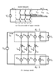
[0010] FIG. 3 shows an example circuit model of an upper module (a) and
and an average model of a dual inverter integrating identical DC sources. In
some embodiments, switch averaging can model each of the six half-bridges
as an ideal voltage source.
[0011] FIG. 4 shows Phase "a" voltage and current waveforms ford = 0.53.
[0012] FIG. 5 shows a chart illustrating a normalized inductor current ripple.
In some embodiments, inductor current ripple size varies with conversion
ratio, where Vo = V1 = V2. When each battery pack has nominal voltage near
the input DC voltage, the operating region near 1:1 voltage ratio may
achieve optimal ripple reduction.
[0013] FIG. 6 shows an example complementary and interleaved switching
sequence for inner switches operated at d = 0.53. di., and d21 are mapped to
inner switches S11 and S21, respectively. The most significant harmonic
frequencies are shown.
[0014] FIG. 7 shows a comparison of i1 with and without interleaved
switching, at d = 0.53. Phase currents in the top plot overlap when
interleaving is not applied. Interleaved switching increases the ripple
frequency and reduce peak-to-peak ripple.
[0015] FIG. 8 shows an example control diagram for controlling current.
[0016] FIG. 9 shows example simulation results of constant current control
with sref step from 22 A to 44 A. Difference between
-out]. and Lutz is due to
voltage balancing controller acting on voltage mismatch.
[0017] FIG. 10 shows example simulation results of voltage balancing control.
V1 and V2 have a 7V deviation at t = 0.
[0018] FIG. 11 shows example simulation results of switching ripple in i
=s,abcf
idcf Ii, and i2, showing cancellation of most significant harmonic(s).
- 3 -
CA 2983328 2017-10-23
[0019] FIGS. 12A and 12B show an example laboratory prototype of 11 kW
dual inverter charger with a salient-pole rotor mimicking a permanent-
magnet rotor. FIG. 12A shows a circuit diagram and FIG. 23B shows an
experimental setup.
[0020] FIGS. 13A and 13B show example experimental results of constant
current control at operating points (a) V1 = V2 = 175V , VC = 230V and (b)
V1 = V2 = 245V , VC = 230V . The input current is initially stepped up to its
rated value (45 A), and then stepped down by 50% at t = is.
[0021] FIGS. 14A and 14B show example experimental results of switching
ripple for 'dc, is,abcf ilf and i2 using the described example switching
method.
FIG 14A is a current waveform, and FIG. 14B is a Fourier spectrum of current
ripple.
[0022] FIG. 15 shows example experimental result of voltage balancing
control. Supercapacitor banks are pre-charged with 7V deviation, and
controller regulate Ad to achieve voltage balance.
DESCRIPTION OF EXAMPLE EMBODIMENTS
[0023] To address charger complexity, combined traction and charging
systems have been studied extensively in the past decade. The concept is to
configure on-board traction components for charging, thus eliminating or
greatly reducing the complexity of battery chargers. Subotic et al. proposed
an integrated charger based on a 9-phase traction system [5]. As shown in
Fig. 1(a), the machine's neutral points can be directly connected to a three-
phase AC input, thus requiring no additional hardware between the AC grid
and traction system. This topology also produces no net torque for vehicle
propulsion in the charging process. Other multiphase machines for integrated
charging are summarized in [6]. In terms of integrated charging via single-
phase AC systems, Fig. 1(b) shows the topology proposed by Pellegrino et at.
It employs the traction system as a PFC boost converter, which is interfaced
to a single-phase AC source via rectifier [7]. In Fig. 1(c), Tang et at. used
a
- 4 -
CA 2983328 2017-10-23
set of parallel-connected traction inverters and two motors to charge from a
single-phase AC source and thereby eliminates the need for the rectifier [8].
In either topology, the charger requires no additional dc/dc converters, thus
addressing weight, volume, and cost considerations of the EVSE. However, in
both cases the minimum allowable battery voltage must always exceed the
peak voltage of the AC mains.
[0024] The integrated chargers previously discussed are specifically for
single-
phase or three-phase AC systems. Due to the rapid penetration of
renewables, grid-connected storage and DC-supplied loads, there is already
significant effort in integrating DC micro grids within existing AC networks
[9]. Ideally future EV chargers would accommodate charging from both
existing DC fast chargers as well as from DC microgrid networks.
[0025] In some embodiments described herein, an integrated charger can
offer, in some situations, electric vehicle fast charging from emerging DC
distribution networks. It leverages the existing dual inverter drive to
operate
as aforementioned integrated chargers, with the added benefits of improved
voltage range and harmonic performance. The dual inverter traction system
may, in some situations, provide increased speed range and battery
integration without use of dc/dc power converters or additional magnetic
materials, thus may offer an efficient and light-weight solution attractive
for
electric vehicles. Although two inverters are required, there is marginal
increase in cost because each inverter stage is rated for half the total
processing power. The dual inverter can, in some situations, facilitate power
transfer between two isolated DC sources and the open-ended windings of
the motor via differential connection of two voltage source converters. From
previously proposed applications of the dual inverter for all-electric
vehicles,
the energy source is either a split-battery pack or a battery and floating
capacitor bridge [11], [12]. The dual inverter configuration may, in some
situations, offer voltage boost from the secondary inverter to enable high
speed operation, improved efficiency at high speed, modular battery
installation, and hybrid energy storage integration [10]-[15].
- 5 -
CA 2983328 2017-10-23
[0026] A challenge associated with the dual inverter drive is the need to
charge two independent batteries. Hong et. al demonstrated that a single
charger could be utilized for charging both batteries [16]. Shown in Fig.
1(d),
the primary battery is charged using a standalone charger, while the
secondary battery is charged from the first via the traction system.
[0027] In some embodiments, the present application describes a means
which may, in some instances, eliminate the standalone charger in cases
where DC power network access is available. The topology can be backwards
compatible to conventional DC fast charging infrastructure. The proposed
charger in this work is shown in Fig. 1(e). Contrary to other integrated
chargers discussed earlier, placing the DC input at the differential
connection
of the traction system may enable rapid charging of dual storage media
without a standalone charger. The topology may address the limited voltage
range in the single inverter charging systems by using the series connection
of two traction inverters, thus providing charging functionality even when the
battery is at low state-of-charge. While the embodiments described below
focus on vehicle charging, in some embodiments, the topology can be
capable of bi-directional energy exchange with an external DC power
network.
[0028] In some situations, embodiments of the present application may
provide: an integrated charger suited for emerging DC networks, where fast
charging is enabled by direct connection to a DC source; improved input
voltage range using differential connection of dual inverter topology,
requiring no external hardware; and/or a switching method utilizing
complementary and interleaved phase shift to improve harmonic
performance compared to single inverter systems.
[0029] The new architecture may offer rapid EV charging from the emerging
DC grid with the potential to reduce charger cost, weight, and complexity by
integrating charging functionality into the traction system.
TOPOLOGY
- 6 -
CA 2983328 2017-10-23
[0030] An example DC charging configuration is shown in Fig. 2. For the
purpose of this paper, switches, voltage and current quantities for the upper
and lower modules are labeled "1" and "2", respectively. The EV battery
pack, consisting of n-strings, is split evenly between a pair of 2-level
voltage
source inverters. Each battery string has the same number of cells per string,
thus maintaining the same nominal voltage as the combined battery pack.
The AC side is connected to the open-ended windings of the electric motor
such that the machine leakage inductance is shared between the two switch
networks.
[0031] A feature of the example dual inverter drive not previously exploited
is
its ability to leverage differential connections for EV charging. The DC
terminals tap off the high-side of module 1 and low-side of module 2. Power
can be fed directly from a DC microgrid without a dc/dc intermediate stage.
Each set of 3 half-bridge switch networks is connected in a cascaded manner
with the DC input and batteries to account for any voltage mismatch. In
addition, the dual battery pack enables doubling of the motor voltage. Unlike
the single traction-based integrated charger in Fig. 1(b), this permits
charging even when the voltage in each battery pack is less than the DC
input voltage. This may be crucial for future trends in bulk power transfer,
where fast charging stations are expected to support up to 1000 V at the
vehicle inlet [3], [17].
[0032] Another potential benefit of utilizing two traction inverters is
current
ripple reduction. Since the motor leakage inductance, Ls, is limited by the
magnetics of the EV motor, it is beneficial to minimize potentially high
ripple
component via controls. Thus, two types of switching methods are deployed.
The combination of 180 . phase shift between upper/lower cells, and 120 .
interleaving between parallel phases both reduce switching ripple in , and
Complementary switching is not feasible for the integrated charger in Fig.
1(b).
- 7 -
CA 2983328 2017-10-23
[0033] Power transfer between the DC input and each battery unit is achieved
by regulating the inductor currents. Its principle of operation is akin to the
single string multi-port dc/dc converter developed in [18], however, the
developed converter is reconfigured for 3-phase motor drives in this work.
OPERATION
[0034] In some embodiments, the dual inverter is configured to operate as a
set of dc/dc converters in charging mode, as opposed to performing dc/ac
conversion in traction mode. Its principle of operation is analyzed via the
average model depicted in Fig. 3. This section also highlights the impact of
complementary and interleaved switching on harmonic performance.
A. Average Model
[0035] The average model of the dual inverter is developed for identical
energy storage integration, as in the case of the split-battery pack. Battery
pack balancing will be addressed in Section IV. A dynamic model of the half-
bridge network for a multilevel converter was developed in [19], but can also
be used to represent the average switch model. Each of the six half-bridge
converters is modeled as an ideal, controlled voltage source. The voltage
depends on the duration in which the storage unit is inserted. The battery
currents, il and i2, are derived from power balance. Although power flow can
be bidirectional, this work identifies Vdc as the input and V1 & V2 as
outputs.
[0036] In Fig. 3(a), each half-bridge is modeled as:
= ( 1)
V2i = (2)
where i = {a, b, c} for 3 interleaved dc/dc stages.
[0037] Only the switch network in the upper module is shown because the
two inverters are identical, except V21 is the average voltage measured across
the bottom set of switches instead of the top. As shown in (1) and (2), the
- 8 -
CA 2983328 2017-10-23
duty cycle regulates the duration in which each battery voltage, V1 and V2, is
inserted. Thus, the average voltage across each set of switches is a fraction
of the associated battery voltage. Switch averaging for a single half-bridge
was also discussed in [20].
[0038] Note that the following relation
= d1 (3)
(12 = (19i (4)
is valid for this analysis assuming identical half-bridge switch networks top
and bottom.
[0039] Applying KVL to any arbitrary phase (neglecting losses), the voltage
conversion ratio is
VdC = V. 11i (5)
Assuming d11 = c12; = d for an idealized symmetric system yields:
Vde= (Vl +1/2)d (6a)
TABLE I. Switching States
59i Upper module Lower module
on on insert insert
on off insert bypass
off on bypass insert
off off bypass bypass
+ V9
(6b)
Vde
[0040] Notice the conversion ratio is similar to that of the boost converter,
>
suggesting l+V2 'I( to enable boost operation. This is not a limiting
- 9 -
CA 2983328 2017-10-23
factor for EV charging because the charging station's DC output voltage is 60
V to 500 V [3], and each string of EV battery cells spans from 300V to 500V
[21]. By assigning one battery string to each module, the minimum output
voltage always exceeds the input voltage. Furthermore, the battery
management system shall not permit the battery to discharge below the
minimum voltage specified by the manufacturer.
[0041] Figure 3 also shows that the DC input current is the sum of the
inductor currents:
= isa isb se (7)
Output currents i and i2 can be derived from power balance:
i1/ui = di Usti isb isc) (8a)
= (8b)
i2 = idc(12 (8c)
where i1 and i2 are fractions of the DC input current set by the duty cycle in
each module.
[0042] Using (8), the average power supplied to each battery pack is
= V d (9a)
P.) =V2ith.d9 (9b)
The average current into the battery is thus a function of the combined stator
currents and duty cycle. Through proper switching action of the half-bridge
switch networks, the proposed charger can effectively control the individual
battery pack currents.
B. Switching Sequence
- 10 -
CA 2983328 2017-10-23
,
,
[0043] For the remainder of this paper, d11 and d21 are mapped to inner
switches SI., and S2i, respectively. For instance,
1.
5,1 a , ( t. ) = 01 1 r (10)
,t, < d1 õ Tsõ,
{
u , alai sw < t < Tsui
[0044] 1) Complementary switching: A complementary strategy is applied to
switches between the upper and lower modules. Thus, the following analysis
examines the impact of complementary switching on phase "a". Gating
signals for the inner switches, Vsa' isa' ila' and i2a are shown in Fig. 4.
Under
balanced load conditions, each pair of "inner" and "outer" switches have the
same percentage on-time in one switching period. However, the gating
.
pulses between the two modules can be phase-shifted by 180 as
demonstrated in [18]. This strategic overlap of gating pulse reduces the
energy variation in the inductor, resulting in half the ripple current at
twice
the switching frequency.
[0045] The peak-to-peak inductor current ripple for V1 = V2 = Vo (idealized
symmetric system) is
(Vic ¨ -17,) _____________________________ di T., ,,
, (11a)
L,
V i T . , 1 17
A : = ( ( ,s a ( 1 Vo c) ( 1 A v dc
(lib)
where the second expression is derived by combining (6b) and (11a).
Plotting (11b) in Fig. 5, this expression highlights one of the key features
of
this topology: the inductor energy variation, or current ripple, depends on
the voltage difference Vdc ¨Vo. Notice for the case where the battery packs
are balanced, and V1 = V2 = Vdc, this yields zero inductor current ripple. The
- 11 -
CA 2983328 2017-10-23
ideal operating range is centered around Vde to
minimize distortion in
the supply lines.
[0046] The branch current of i1 and i2 from any arbitrary phase, denoted by
pulsates due to the discontinuous conduction of the switch network:
= (12)
12i = isiS2i (13)
Notice that the inductor ripple also propagates into the battery. Since the
inductor ripple is negligible relative to the pulsating current generated by
summing the branch currents, complementary switching has minimal effect
on the battery currents. Thus, to minimize current harmonics in the
batteries, interleaved switching between parallel phases is used. The
proposed switching method also reduces the switching ripple at the DC input.
[0047] 2) Interleaved switching: This switching strategy has not been
previously studied in an integrated charger based on the dual inverter. As
shown in Fig. 6, the gating pulses between phase a, b, and c are phase
shifted by 120 . This further reduces the peak ripple observed in idc. Due to
the phase-shift of stator currents, the peak-to-peak 'dc is approximately 1/3
of the ripple generated using in-phase switching, and the most significant
switching component is shifted to the 6th harmonic.
[0048] Figure 7 shows the impact of phase interleaving on output currents
and i2. As discussed previously, the currents in all switches are "chopped"
regardless of the switching pattern. The unfiltered battery currents are the
sum of the pulsating currents in the inner switches:
== ila -F ilb ;lc (14)
i2 " i2a -11r- i9b -F 12c (15)
- 12 -
CA 2983328 2017-10-23
[0049] To minimize the switching ripple due to discontinuous conduction,
interleaved switching enables continuous conduction of
ii and i2 for < d < 1- . The battery currents conduct through at least one
of the 3 phases. The third plot in Fig. 7 shows that at d = 0.53, interleaving
results in approximately of the ripple component, and the most significant
harmonic is shifted to 3fsw. The contribution of the inductor current ripple
to
the total harmonic distortion in i1 and i2 is negligible at this operating
point.
[0050] In summary, the proposed switching sequence produces
Ais,abc, /id, and ii,2 at 2f8w,6f8w, and 3fsw, respectively. This effectively
leads
to reduced THD and semiconductor losses. Reduction in peak-to-peak output
current ripple also helps to prevent battery capacity fade and impedance
degradation [22].
[0051] Recall that an ideal, symmetrical system having balanced energy
sources was studied in previous sections. This allows the controller to set
equal duty cycles to both the upper and lower modules. To address the
scenario where the isolated battery packs have a different state-of-charge
during the charging process, the duty cycles are decomposed into sum and
difference terms, defined as:
di 1
¨ Ed
75
-= d9 T ( 1 6)
75 Ad
[0052] In some instances, the objective of the DC charger may be to 1)
regulate the DC inductor current using the sum component 2) equalize the
stored energy in the split energy source using the difference component.
Note that coupling between the two terms may be present.
A. Inductor current control
[0053] In Fig. 8, three PI controllers are implemented for constant current
control of parallel phases. Since the EVSE typically regulates the DC current
- 13 -
CA 2983328 2017-10-23
at the vehicle inlet, each inductor current will track one-third of the DC bus
current reference.
[0054] An expression for the dynamics of the system is developed by applying
KVL to the average model:
al
Vde d /7.42i + isiRs + Ls __ = 0 (17a)
(It
Vdc (vt __ +9142 )Edi (1/1 V2),Adi
'Si 17b)
Rs +
where d1, and d21 have been replaced by Id and Ad as per (16). Ideally, if the
battery voltages are balanced, then only the sum term drives the DC current.
However, the difference term is coupled to the current controller. To avoid
stability issues, voltage balancing controller can be designed to have
significantly slower response to voltage dynamics. Thus, (V1¨ V2) Ad, can be
regarded as a DC offset in the time scale of the current controller.
[0055] The example controller discussed in this work is developed for constant
current charging. The control scheme for constant voltage charging may be
investigated in future works.
B. Energy balancing
[0056] In Fig. 8, the voltage balancing controller takes the voltage
difference
and outputs Ad, which is then subtracted from d11 and added to d2i=
Therefore, if the DC source in the upper module is overcharged relative to
the lower, then the lower one will be inserted more frequently. Both sources
are charged simultaneously but with an offset to shift the power distribution.
To ensure this offset does not exceed the operating limits of the converter, a
limiter is implemented at the output of the voltage balancing controller. Note
that the balancing controller uses voltage to extrapolate the total stored
energy in the DC source. Other parameters may be used for energy
management, such as comparing state-of charge (Coulomb count) of a split-
battery pack.
- 14 -
CA 2983328 2017-10-23
SIMULATION RESULTS
[0057] A full-switch model of the proposed integrated charger is implemented
in MATLAB/SIMULINK with a PLECS toolbox. The circuit diagram is shown in
Fig. 12(a), and simulation parameters are listed in Table II.
TABLE II. Simulation Parameters
Parameter Symbol Value
Input power 50k W
Power/module P1, P9 25kW
DC bus voltage Vdc 380V
Initial SC voltage VI, V2 360V-365V
DC bus current idc 132A
Stator current is,abe 44A
Capacitance/SC bank c,õõ1, C9 16.6 F
Output capacitors Cl C2 9.6MF
Stator inductance , 0.8 rn I-1
Stator resistance R
Switching frequency f 7.5k Hz
[0058] In place of EV batteries, two supercapacitor banks are used in this
simulation study to mirror the experimental system. The faster
charge/discharge rates of the supercapacitor vs. a battery facilitates a less
time consuming study of storage energy balancing algorithms. All current
quantities are positive in the direction indicated by the arrow, which shows
power transfer from the DC input to supercapacitors. This simulation study
demonstrates
= Current control and voltage balancing functionality
= DC charging at operating point V1 < Vdc, V2 < Vdc, which is one
limitation of previously proposed integrated chargers
= Current ripple reduction using proposed switching method
-15 -
CA 2983328 2017-10-23
TABLE III. Experimental Parameters
General Parameters Symbol Value
Input power 'dc 10.35kW
Power/module P.1., P2 5.17k1V
DC bus voltage 230V
Case #1: 171 < Vdc, V2 < Vdc
Initial SC voltage V1. V2 175V
Case #2: V1 > V. V2 > Vdc
Initial SC voltage Vit ,11;, 245V
DC bus current idc .45A
Stator current is,abc 15A
Capacitance/SC bank Csci Csa 16.6F
Output capacitors C2 9.6m F
Switching frequency fs 7.5kHz.
Machine Parameters Symbol Value
Power Prated
Line-to-line voltage Vrated 2201'
Line current irated 39.4.1
Stator inductance U.5m 1.1
Stator resistance Ps
Rotor excitation current if 5A
[0059] 1) Constant current control: Fig. 9 shows the system response when a
current step is applied at t = 0.1s. The inductor reference current, i
-sref is
stepped from 22 A to 44 A. This allows the total input power, DC bus current,
and current into the supercapacitors to double accordingly. Id initially
drops,
as derived in (17b), to act on the increase in current demand and settles to
its new value in 10 ms. After the transient, the charger operates at rated
conditions (50 kW), which is the typical system rating for the CHAdeM0 EVSE
[23].
[0060] 2) Voltage balancing: Fig. 10 demonstrates the effect of voltage
balancing control on energy distribution. The super-capacitor banks have a 7
V difference at t = 0, and achieves energy balance when V1 = V2. The delta
term, Ad, regulates the rate of convergence. The voltage balancing response
can also be observed in Fig. 9, where iout1 and iout2 are regulated such that
P1 = 18kW and P2 = 32kW. If supercapacitors are balanced, then Ad = 0 to
deliver 25 kW to each module.
- 16 -
CA 2983328 2017-10-23
[0061] 3) Harmonic analysis: Fig. 11 verifies the harmonic decomposition of
is,abc, LC/ ti 1 and
12 for the balanced voltage operating scenario. The most
significant harmonic frequencies in the inductors, DC bus, and supercapacitor
prior to filtering are 2fsw, and
3fsw, respectively. Observe that for i1 and
i2, the 6th harmonic from idc propagates to the output. However, it has
negligible impact on output peak-to-peak ripple because the DC current is
significantly larger than the inductor ripple.
EXPERIMENTAL RESULTS
[0062] This section discusses experimental testing of an 11 kW laboratory
prototype based on the proposed charger topology. One of the most
commonly adopted DC fast chargers (CHAdeM0) is rated at 50 kW. In this
work, the system rating is scaled-down to verify basic charging functionality
using a dual inverter powertrain. Experimental results show constant current
control, voltage balancing, and switching ripple reduction in a wide operating
region. Charging at two operating points will be validated: 1) V1 < Vdc, V2 <
Vdc, and 2) V1 > Vdc, V2 > Vdc. In either case, the system is operating at
94% of the rated power of the motor.
[0063] The laboratory setup is shown in Fig. 12, and system parameters in
Table III. A Regatron power supply provides 230 V at the DC input, where
the terminals represent the charging inlet of the vehicle. A 0.5 kWh
supercapacitor bank is connected to each 2-level VSC. Each supercapacitor
bank consists of 180 series-connected cells with 3000 F per cell. Thus, each
string has total capacitance of 16.6 F. Permanent magnet synchronous
motors (PMSM) and induction motors are the most commonly used electric
motors in EVs. Thus, the wound rotor SM in the prototype is operated with
constant field, similar to a PMSM. This is achieved by exciting the rotor
windings to ensure rotor flux is present. The impact of rotor saliency on
phase current ripple discussed below.
[0064] The control strategy in Fig. 8 can be implemented on a real-time linux
PC controller with integrated FPGA.
- 17 -
CA 2983328 2017-10-23
[0065] A. Case #1: Charging at V1 < Vdc, V2 < Vdc
[0066] Figure 13(a) shows experimental results of constant current control
when each supercapacitor voltage is less than the input voltage. This is
analogous to charging a high-energy, low-voltage EV battery pack, or
batteries at low state-of charge. The results demonstrate functionality of the
controller when isref is stepped up from 0 to 15 A, and then stepped down to
50% of its rated current. The input current is shown to be the sum of the
phase currents. The combined energy storage system, with 175 V per
supercapacitor bank, charges from a 230 V DC supply at 10.35 kW rated
power, hence charging batteries with power comparable to rated machine
power. Similar to the case presented in simulation, idc and is,abc tracks the
new current reference.
[0067] B. Case #2: Charging at V1 > Vdc, V2 > Vdc
[0068] Figure 13(b) shows experimental results of constant current control
when each supercapacitor voltage exceeds the input voltage. This operating
scenario applies to charging EV batteries designed for high-voltage, high-
speed operation. The input voltage is fixed at 230 V and each supercapacitor
bank charges at 245 V, and the total charging power is also 10.35 kW. The
same current steps are applied to this operating point. As shown in Fig.
14(a), the peak-to-peak ripple between phase currents are not identical. Use
of a salient-pole rotor leads to asymmetry in flux linkage between stator and
rotor, which marginally affects the total inductance per phase.
[0069] C. Voltage Balancing
[0070] Fig. 15 demonstrates the functionality of voltage balancing control.
The supercapacitor voltages prior to charging are 154 V and 147 V. When the
controller is enabled, the DC bus current steps from 0 to 10A, drawing 2.3
kW from the DC supply. Due to the applied offset between dl and d2, the
"undercharged" supercapacitor bank has a faster rate of charge compared to
the "overcharged" supercapacitor bank. The supercapacitor voltages
- 18 -
CA 2983328 2017-10-23
converge at approximately 178 V. The results verify operation of the
balancing controller in response to the initial voltage deviation.
[0071] D. Discussion of Switching Ripple and Rotor Saliency
[0072] Fig. 14(a) shows the switching ripple of idcr is,abcf i1,and i2 for
case #1,
but at lower current reference. This is to show that the magnitude of the
peak-to-peak ripple is independent of the average charging current.
Neglecting switching noise in the current reference step from Fig. 13(a), the
switching ripple between charging at 'dc = 15A and 'dc = 45A is identical.
Comparing the Fourier spectrum of the simulation and experimental study,
the switching ripple at the switching frequency (7.5 kHz) is eliminated in
both
systems. Any discrepancy between simulation and experimental results is
due to differences in operating point, and rotor saliency. For example, output
currents i1 and i2 from laboratory results have higher 6th harmonic than 3rd
in comparison with simulation results, where the 3rd harmonic is dominant.
This is due to the fact that the simulation model is operated at rated
conditions. In the experimental work, charging at low currents introduces
higher 6th harmonic ripple.
[0073] Also note that isb ripple components in Fig. 14 are noticeably smaller
than the other two phases. This results from using a salient-pole rotor, where
the phase inductance depends on the rotor's electrical position [7]. In the
experimental results, the rotor was arbitrarily oriented to produce the
asymmetric phase current ripple in Fig. 14(a). In Fig. 14, difference in phase
current ripple increases the 2nd harmonic component in 'dc. However, the 6th
harmonic is shown to be the dominant switching component in the input
current.
[0074] Some embodiments of the present application present a new
integrated charger topology that may offer direct charging from the DC grid
without any off-board hardware. The concept is to connect the vehicle
charging input to the differential ends of the dual traction system. Although
a
- 19 -
CA 2983328 2017-10-23
=
second converter is required, higher motor voltages and lower currents may
be utilized, and the net switch VA rating remains unchanged.
[0075] In some instances, the proposed integrated charger based on the dual
inverter has been demonstrated to enable charging over a wide voltage
range. An 11 kW laboratory prototype verifies DC charging for supercapacitor
voltages V1 and V2 above and below the DC input voltage. Furthermore,
results show effective current control and energy balancing amongst the two
supercapacitor banks, which are used in place of batteries to reduce
experimental run-time. The proposed switching method may, in some
instances, attenuate significant switching harmonics, which is essential for
addressing the use of limited motor inductance as interface inductors. The
control method for constant voltage charging will be studied in future works.
In practice, the proposed topology's charging rate is limited by thermal
constraints of the motor and traction power electronics, thus highlighting its
ability to charge at the rated power of the traction system ideal for electric
vehicle fast charging.
- 20 -
CA 2983328 2017-10-23
REFERENCES
[1] R. Schmidt, "Information technology energy usage and our planet," in
11th Intersociety Conf. on Thermal and Thermomechanical Phenomena in
Electronic Systems, vol., no., pp.1255-1275, 28-31 May 2008.
[2] M. Yilmaz and P. T. Krein, "Review of charging power levels and
infrastructure for plug-in electric and hybrid vehicles," 2012 IEEE
International Electric Vehicle Conference (IEVC), Greenville, SC, 2012, pp.
1-8.
[3] Electric Vehicle Conductive Charging System Part 23: DC Electric Vehicle
Charging System, IEC 61851-23, 2014.
[4] M. Smith, J. Castellano, "Costs Associated With Non-Residential Electric
Vehicle Supply Equipment - Factors to consider in the implementation of
electric vehicle charging stations," U.S. Department of Energy Vehicle
Technologies Office, Nov. 2015.
[5] I. Subotic, E. Levi, M. Jones and D. Graovac, "On-board integrated
battery chargers for electric vehicles using nine-phase machines," 2013
International Electric Machines & Drives Conference, Chicago, IL, 2013,
pp. 226-233.
[6] I. Subotic, N. Bodo, E. Levi, B. Dumnic, D. Milicevic and V. Katic,
"Overview of fast on-board integrated battery chargers for electric
vehicles based on multiphase machines and power electronics," in IET
Electric Power Applications, vol. 10, no. 3, pp. 217-229, 3 2016.
[7] G. Pellegrino, E. Armando and P. Guglielmi, "An Integral Battery Charger
With Power Factor Correction for Electric Scooter," in IEEE Transactions
on Power Electronics, vol. 25, no. 3, pp. 751-759, March 2010.
[8] Lixin Tang and G. J. Su, "A low-cost, digitally-controlled charger for
plug-in hybrid electric vehicles," 2009 IEEE Energy Conversion Congress
and Exposition, San Jose, CA, 2009, pp. 3923-3929.
[9] K. Shenai and K. Shah, "Smart DC micro-grid for efficient utilization of
distributed renewable energy," IEEE 2011 EnergyTech, Cleveland, OH,
2011, pp. 1-6.
-21 -
CA 2983328 2017-10-23
[10] D. M. Vilathgamuwa, S. D. G. Jayasinghe, F. C. Lee, U. K. Madawala, "A
unique battery/supercapacitor direct integration scheme for hybrid electric
vehicles," in IECON 2011 - 37th Annual Conference on IEEE Industrial
Electronics Society, vol., no., pp.3020-3025, 7-10 Nov. 2011.
[11] D. Casadei, G. Grandi, A. Lega; C. Rossi, "Multilevel Operation and
Input Power Balancing for a Dual Two-Level Inverter with Insulated DC
Sources," IEEE Trans. on Ind. Applicat., vol.44, no.6, pp.1815-1824,
Nov.-dec. 2008.
[12] Y. Lee and J. I. Ha, "Hybrid Modulation of Dual Inverter for Open- End
Permanent Magnet Synchronous Motor," in IEEE Transactions on Power
Electronics, vol. 30, no. 6, pp. 3286-3299, June 2015.
[13] Junha Kim, Jinhwan Jung and Kwanghee Nam, "Dual-inverter control
strategy for high-speed operation of EV induction motors," in IEEE
Transactions on Industrial Electronics, vol. 51, no. 2, pp. 312-320, April
2004.
[14] R. U. Hague, A. Kowal, J. Ewanchuk, A. Knight and J. Salmon, "PWM
control of a dual inverter drive using an open-ended winding induction
motor," 2013 IEEE 28th Annual Applied Power Electronics Conference and
Exposition (APEC), Long Beach, CA, USA, 2013, pp. 150-156.
[15] S. Lu, K. A. Corzine and M. Ferdowsi, "A Unique Ultracapacitor Direct
Integration Scheme in Multilevel Motor Drives for Large Vehicle
Propulsion," in IEEE Transactions on Vehicular Technology, vol. 56, no. 4,
pp. 1506-1515, July 2007.
[16] J. Hong, H. Lee and K. Nam, "Charging Method for the Secondary
Battery in Dual-Inverter Drive Systems for Electric Vehicles," in IEEE
Transactions on Power Electronics, vol. 30, no. 2, pp. 909-921, Feb.
2015.
[17] Plugs, socket-outlets, vehicle connectors and vehicle inlets - Conductive
charging of electric vehicles Part 3: Dimensional compatibility and
interchangeability requirements for d.c. and a.c./d.c. pin and contact-tube
vehicle couplers, IEC 62196-3, 2014.
- 22 -
CA 2983328 2017-10-23
[18] Yuanzheng Han, M. Ranjram, P. W. Lehn, "A bidirectional multi-port DC-
DC converter with reduced filter requirements," in 2015 IEEE 16th Workshop
on Control and Modeling for Power Electronics (COMPEL), vol., no., pp.1-6,
12-15 July 2015.
[19] G. J. Kish, C. Holmes and P. W. Lehn, "Dynamic modeling of modular
multilevel DC/DC converters for HVDC systems," 2014 IEEE 15th Workshop
on Control and Modeling for Power Electronics (COMPEL), Santander, 2014,
pp. 1-7.
[20] H. Ban arnklau, A. Gensior and S. Bernet, "Derivation of equivalent
submodule per arm for modular multilevel converters," 2012 15th
International Power Electronics and Motion Control Conference (EPE/PEMC),
Novi Sad, 2012, pp. LS2a.2-1-LS2a.2-5.
[21] Siang Fui Tie and Chee Wei Tan, "A review of energy sources and
energy management system in electric vehicles," Renewable and Sustainable
Energy Reviews, Volume 20, Pages 82-102, April 2013.
[22] Clark G. Hochgraf, John K. Basco, Theodore P. Bohn, Ira Bloom, "Effect
of ultracapacitor-modified PHEV protocol on performance degradation in
lithium-ion cells," Journal of Power Sources, vol.246, pp.965-969, January
15, 2014
[23] IEEE Standard Technical Specifications of a DC Quick Charger for Use
with Electric Vehicles, IEEE Std. 2030.1.1, 2015.
- 23 -
CA 2983328 2017-10-23